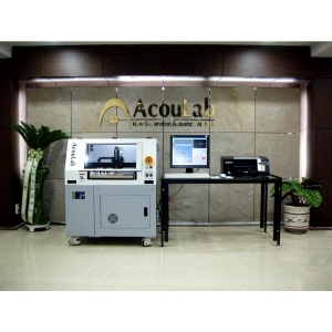
Company
Established in 1998, AcouLab Co., Ltd. is a venture company specializing in ultrasonic inspection equipment. We develop and manufacture a wide variety of industrial ultrasonic inspection systems, including world-class Ultrasonic C-Scan Systems, Scanning Acoustic Microscopes (SAM) for semiconductor inspection, Ultrasonic Phased Array Systems, and Time of Flight Diffraction (TOF) Systems for weld inspection.
Equipped with extensive experience and accumulated know-how, our R&D personnel develop and manufacture ultrasonic devices tailored to customer needs, ranging from research equipment to fully automated inspection systems for production lines.
AcouLab Co., Ltd. aims to help improve our customers' product quality, increase productivity, and reduce costs by providing comprehensive solutions related to non-destructive testing using ultrasound, in addition to the development and manufacturing of inspection systems.
We will always strive for customer satisfaction through the world's best technology and quality.
All Employees of AcouLab Co., Ltd.
Product
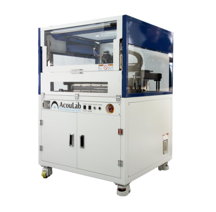
SAM-DENEB
• Standard SAM
• Surface and internal defects, size, and location measurement
• Max 1000mm/s Scan Speed
• Scan Area : 350mm*150mm
• Application : Flip Chip, BGA, QFT, TBGA, FBGA, SOP, FET, MLCC, PCB
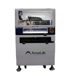
SAM-VEGA
• Standard SAM
• Surface and internal defects, size, and location measurement
• Max 1000mm/s Scan Speed
• Loading/Unloading System
• Scan Area : 350mm*150mm
• Application : Flip Chip, BGA, QFT, TBGA, FBGA, SOP, FET, MLCC, PCB
SAM-MINI
• Compact SIZE SAM
• Internal defect inspection of semiconductor packages
• Max 750mm/s Scan Speed
• Scan Area : 320mm*180mm
• Application : Flip Chip, BGA, QFT, TBGA, FBGA, SOP, FET, MLCC, PCB
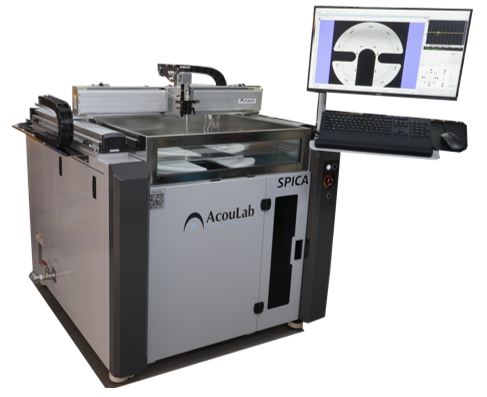
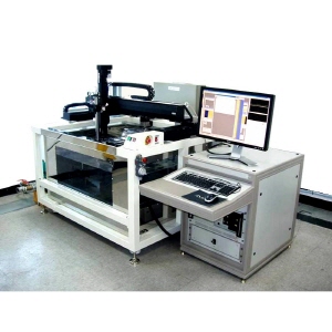
SAM-SPICA
• Medium Size SAM
• Max 1000mm/s Scan Speed
• Scan Area : 750mm*750mm
• Application : ESC, ITO, Heater
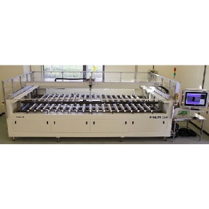
SAM-ATHLON
• Large Size SAM
• Max 1000mm/s Scan Speed
• Scan Area(Max) : 4000mm*2500mm
• Application : Large Size Flat and Circular LCD/PDP, ITO Target
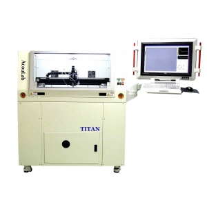
SAM-TITAN
• Medium Size SAM
• Max 1000mm/s Scan Speed
• Water Tank Up/Down Support
• Scan Area(Max) : 750mm*750mm
• Application : semiconductor, PCB, Material, etc.
SAM-CYGNUS
• Wafer Auto Inspection
• Wafer Map, Barcode, Wafer Pre Aligner, Spin Coater
• Waterfall System
• Scan Area(Max) : 4"~6" Wafer
• Application : Wafer
SAM-ITS
• Industrial SAM
• Immersion Tank System
• Scan Area : Customized
• Application : ITO Target, STEEL, TUBE, BAR, Composite materials, etc.

Pulser&Receiver
• BandWidth : 1~500Mhz
Application


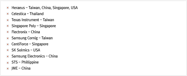
Customer
Customer List
CONTACT
Email : sales@acoulab.co.kr
TEL : 032-676-8077~8
Address : 8, Sudo-ro 55beon-gil, Ojeong-gu, Bucheon-si, Gyeonggi-do, 14516, Rep. of KOREA (Bucheon Center)
Address : M1004, 32, Songdogwahak-ro, Yeonsu-gu, Incheon, 21984, Rep. of KOREA (Songdo Center)